Overview
This study, co-authored by Jungmok Seo (then at the Nanobio Device Laboratory, School of Electrical and Electronic Engineering, Yonsei University), who now leads the BLISS Lab at Yonsei University, used a wet-chemistry galvanic displacement reaction to deposit palladium nanoparticles selectively on defects in chemical vapor deposition (CVD) graphene. The sheet resistance decreased from approximately 1 kΩ/sq to 173 Ω/sq at 91.3% transmittance, and a transparent heater made from palladium-decorated graphene with 154 Ω/sq reached 94.4 °C at 12 V, compared with 60.6 °C for pristine graphene.
Background
CVD graphene can be produced at industrial scale, but the growth process leaves grain boundaries, wrinkles and cracks that raise the sheet resistance of single-layer graphene above 1 kΩ/sq, far from the theoretical value of approximately 30 Ω/sq. Earlier routes to improve transport, such as enlarging grains, bridging grains with metal nanowires or selective atomic layer deposition, require sophisticated treatments, high-cost equipment and long processing times. A simpler solution-based method that filled cracks with metal nanoparticles did not address grain boundaries or wrinkles.
Design and approach
Graphene grown on copper foil is immersed in an aqueous PdCl2 solution while still on the foil. In this graphene-buffered galvanic displacement reaction, the copper underneath acts as the anode and dissolves, and the graphene acts as the cathode that supplies electrons for palladium reduction. Defect sites are chemically less stable than the basal plane, so at low PdCl2 concentrations palladium nucleates preferentially at grain boundaries, wrinkles, regions above copper fatigue cracks and exposed edges of multilayer islands. The deposition pattern therefore serves both to decorate and to visualize the defects.
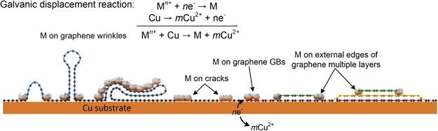
The figure shows galvanic decoration at defect sites in graphene on copper.
Juree Hong, Jae-Bok Lee, Sanggeun Lee et al. “A facile method for the selective decoration of graphene defects based on a galvanic displacement reaction”. Figure 5. DOI: 10.1038/am.2016.42. CC BY 4.0. Figure content is unchanged.
Source figure and caption ↗ · DOI: 10.1038/am.2016.42 ↗ · CC BY 4.0 ↗
How it was evaluated
The authors varied PdCl2 concentration between 0.01 and 5 mM and reaction time, and examined the deposits by field-emission scanning electron microscopy, spherical aberration-corrected scanning transmission electron microscopy with selected-area diffraction, friction force microscopy and Raman spectroscopy. Sheet resistance was measured by the four-probe method together with optical transmittance. Transparent heaters (20 mm × 20 mm) made from pristine and palladium-decorated graphene were driven at a constant 12 V and monitored with an infrared camera, including under bending with a 10 mm curvature.
Key results
Deposition selectivity depended on concentration. A 5 mM solution for 5 min produced a continuous palladium film, deposition above 0.5 mM was not selective, and selective deposition was observed only below 0.5 mM. The palladium nanoparticles averaged approximately 12 nm in size. Diffraction patterns on either side of the polygonal palladium lines showed different lattice orientations, identifying those lines as grain boundaries. Parallel palladium lines matched the shallow copper fatigue cracks, whose spacing is approximately 200 nm, and palladium lines inside grain-boundary-free single domains showed that wrinkles also act as nucleation sites. On stacked islands, palladium formed only along external edges and not along edges buried under another layer, which allowed the stacking configuration to be traced.
Raman spectra showed only minor changes in D, G and 2D peak intensities, indicating little damage to the lattice. After reaction in 0.1 mM PdCl2 for 10 min, the G peak shifted from 1580 to 1595 cm−1 and the 2D peak from 2680 to 2688 cm−1, which the authors assigned to hole doping by palladium. Under the same condition, the nanoparticles connected into nanowire-like lines and the sheet resistance reached 173 Ω/sq, a decrease of approximately 83%. Transmittance fell from approximately 97% for pristine graphene to 91.3%. For comparison, the authors cited approximately 125 Ω/sq at 97.4% transmittance reported elsewhere for HNO3-doped graphene.
In the heater test at 12 V, the steady-state temperature increased as sheet resistance decreased. A palladium-decorated heater with 154 Ω/sq reached 94.4 °C, whereas the pristine graphene heater reached 60.6 °C. During bending with a 10 mm curvature, the maximum temperature dropped early in the test to 85.6 °C, a decrease of approximately 9%, and then remained stable over continued bending; the authors attributed the drop to detachment of some nanoparticles and increased contact resistance. A test with AgNO3 also produced selective silver deposition at defect sites.
Open questions
The authors noted that palladium patterns alone do not easily distinguish grain boundaries from wrinkles, that the exact stacking configuration of multilayer islands could not be confirmed by friction force microscopy, and that the relative contributions of chemical doping and added conduction paths to the lower sheet resistance could not be separated with their setup.
Related research
Selective metal deposition at graphene line defects by atomic layer deposition
This paper cites selective metal deposition at graphene line defects by atomic layer deposition as an earlier route to defect-selective metal growth. The present study replaces the vapor-phase process with a galvanic displacement reaction in solution, in which the copper growth substrate supplies the electrons for palladium deposition.
Abstract-based introductionRESEARCH NEWS
Research in the news
Unverified candidates and access limits (1)
Unverified candidate · Transparent Heater [2/2] ↗
Sources used in this summary
This summary is based on the open-access publisher PDF of the article, including figure legends. The supplementary figures, tables and videos were not reviewed; the text gives the post-decoration transmittance at 500 nm, whereas the Figure 6 legend states 550 nm.