Overview
This study, co-authored by Jungmok Seo (then at the Nanobio Device Laboratory, School of Electrical and Electronic Engineering, Yonsei University), who now leads the BLISS Lab at Yonsei University, used a single-walled carbon nanotube (SWNT) enriched polymer composite as the active layer of a flexible direct-conversion X-ray detector. At a reverse bias of 150 V, raising the SWNT concentration from 0 to 0.01 wt.% increased the X-ray-induced photocurrent from 2.86 to 10.67 nA, and 0.005 wt.% was identified as the optimum when both sensitivity and signal-to-noise ratio (SNR) were considered.
Background
Inorganic X-ray detector materials such as cadmium telluride, silicon carbide and amorphous selenium offer high detection efficiency, but they are costly, fragile and difficult to make flexible, and thinning the layer for flexibility sacrifices X-ray absorption. Semiconducting polymers can be processed over large areas on flexible substrates, yet in organic direct-conversion detectors the photocurrent is limited because X-ray-induced excitons recombine owing to the low electron mobility of organic materials.
Design and approach
Metallic SWNTs were dispersed in toluene with the conjugated block copolymer poly(styrene-b-paraphenylene) (PS-b-PPP) and mixed with the p-type polymer Super Yellow at SWNT concentrations of 0 to 0.1 wt.%. A 5-μm-thick composite film was drop cast onto a poly(ethylene terephthalate) (PET) substrate with 60 nm Au electrodes and capped with LiF (5 nm) and Al (60 nm). Because the SWNTs have a greater electron affinity than the polymer, electrons move into the nanotubes and holes into the polymer at the SWNT-polymer interface, which separates X-ray-induced excitons before they recombine.
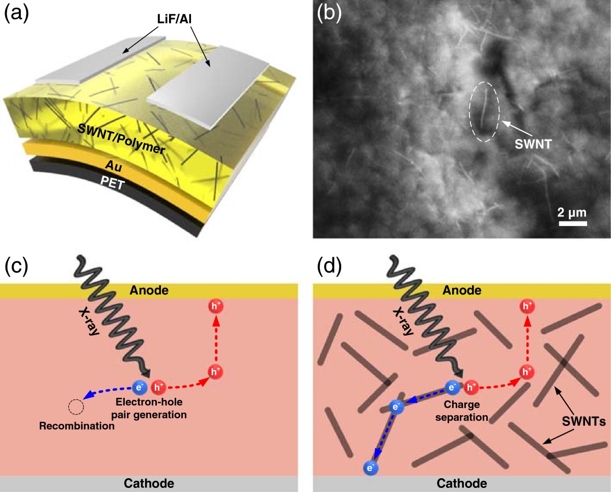
The figure shows the structure and charge-separation concept of a flexible polymer X-ray detector containing single-walled carbon nanotubes.
Heetak Han, Sanggeun Lee, Jungmok Seo et al. “Enhancement of X-ray detection by single-walled carbon nanotube enriched flexible polymer composite”. Figure 1. DOI: 10.1186/1556-276x-9-610. CC BY 4.0. Figure content is unchanged.
Source figure and caption ↗ · DOI: 10.1186/1556-276x-9-610 ↗ · CC BY 4.0 ↗
How it was evaluated
Dispersion was examined by scanning electron microscopy, and devices with a 3 × 3 mm2 active area were characterized by dark current-voltage (I-V) measurements and by photocurrent under an 8.06-keV Kα X-ray beam from a copper target. Photocurrent was recorded as a function of reverse bias and of dose rate, with a 7 mGy/s dose rate and 30 s shutter cycles for the time-dependent response. Sensitivity was calculated from the slope of photocurrent versus dose rate divided by the active volume, SNR was defined as the ratio of photocurrent to dark current, and the 0.005 wt.% device was tested at different bending radii and over repeated bending.
Key results
SEM showed no severe SWNT agglomeration in the composite at 0.1 wt.%. The dark I-V curves remained rectifying up to 0.01 wt.% SWNT, whereas devices above 0.015 wt.% showed ambipolar characteristics, which the authors attribute to the metallic SWNTs dominating conduction. At 150 V and 7 mGy/s, the photocurrent rose from 2.86 nA without SWNTs to 10.67 nA at 0.01 wt.%, about 273% larger. The 0.000 and 0.005 wt.% devices showed saturating photocurrent with bias, while the 0.010 wt.% device did not.
The photocurrent increased linearly with dose rate at 60 V, 90 V and 120 V, following the Fowler model. The 0.010 wt.% device, however, showed a sudden photocurrent increase at -120 V and a non-saturating time-dependent response. From the band diagram, adding SWNTs (work function 4.5 eV) lowered the Schottky barrier heights from 2.3 eV to 0.6 eV for electrons and from 0.8 eV to 0.3 eV for holes, turning the contacts near-Ohmic and allowing space-charge-limited current, which the authors link to the slower and non-saturating response.
At 150 V, the sensitivity was 12.5, 16.9 and 38.9 μC/mGy/cm3 for SWNT concentrations of 0, 0.005 and 0.01 wt.%, respectively. The 0.010 wt.% device, despite the highest sensitivity, had the lowest SNR, approximately 0.18 at -150 V, because the near-Ohmic contacts increased the dark leakage current. The authors therefore selected 0.005 wt.% as the optimal concentration, since it improved both sensitivity and SNR relative to the device without SWNTs.
In the 0.005 wt.% device at 7 mGy/s and 120 V, the dark current showed no discriminable response to the bending radius, while the X-ray-induced current changed slightly. After 1,000 bending cycles at a radius of 0.5 cm, with currents measured every 100 cycles, the device kept a stable X-ray response.
Open questions
The authors state that the gain from SWNTs is limited by the contacts: at high SWNT concentration the reduced Schottky barrier height slows the response, makes it less stable and raises the dark current, so the SWNT content has to be chosen to balance sensitivity against SNR.
Related research
Organic Semiconducting Single Crystals as Next Generation of Low‐Cost, Room‐Temperature Electrical X‐ray Detectors
The related paper’s abstract reports direct X-ray detection at room temperature and stable dose-rate response in organic single crystals. It offers a different charge-transport material strategy from the filled polymer used here.
Abstract-based introductionRESEARCH NEWS
Research in the news
Sources used in this summary
This summary is based on the full text, figure legends and Table 1 of the open-access article (Europe PMC, PMC4493992), checked against the publisher PDF; the supplementary information was not reviewed, and the text cites the conditions of Figure 4a for the bending test in Figure 5b.